Leveraging Optical Chip-to-chip Connectivity to Unleash the Complete Potential of AI
This market research report was originally published at the Yole Group’s website. It is reprinted here with the permission of the Yole Group. Co-packaged optics (CPO) has gained attention recently due to its power efficiency in datacenters. While most leading proponents of CPO targeting networking applications have discontinued CPO programs due to macroeconomic headwinds, the … Leveraging Optical Chip-to-chip Connectivity to Unleash the Complete Potential of AI Read More + The post Leveraging Optical Chip-to-chip Connectivity to Unleash the Complete Potential of AI appeared first on Edge AI and Vision Alliance.

This market research report was originally published at the Yole Group’s website. It is reprinted here with the permission of the Yole Group.
Co-packaged optics (CPO) has gained attention recently due to its power efficiency in datacenters. While most leading proponents of CPO targeting networking applications have discontinued CPO programs due to macroeconomic headwinds, the situation of CPO for artifical Intelligence (AI) and machine learning (ML) systems is different. AI models have an insatiable demand for computing power, storage, and data movement, and traditional architectures are becoming the main bottleneck for scaling ML. As a result, new optical interconnects have emerged for HPC and new disaggregated system architectures, which Yole Intelligence, part of Yole Group reviews in its new report, Co-packaged Optics for Datacenter. In-package optical I/O technology for xPUs, memory, and storage can help achieve the necessary bandwidths. Moreover, the potential for billions of optical interconnects in the future is driving big foundries to prepare for mass production (including silicon photonics process flows) of any PIC architecture from design houses. CPO revenue was about US$38 million in 2022 and is expected to reach US$2.6 billion in 2033, at a 46% CAGR for 2022 – 2033, driven by accelerated data movement in AI/ML gear.

The combination of TeraPHY optical I/O chiplets and SuperNova
 light sources from Ayar Labs delivers dramatically increased bandwidth, at lower latency, over longer distances and at a fraction of the power of existing electrical I/O solutions. Its in-package optical I/O solution is disrupting the traditional performance, cost, and efficiency curves of the semiconductor and computing industries. Martin Vallo, Senior Analyst at Yole Intelligence, had the pleasure of interviewing Terry Thorn, Vice President of Commercial Operations at Ayar Labs, and discussing the current trends in optical interconnects for datacenter applications.
Martin Vallo (MV): We had our last interview in 2021 when you presented your breakthrough optical I/O solution enabling optical communication between computing chips. What is new in the life of Ayar Labs?
Terry Thorn (TT): Over the past 18 months, we have kicked off several high-profile strategic partnerships while also building key relationships with high-volume foundry, laser and supply chain partners. We started 2022 by celebrating a strategic partnership with Hewlett Packard Enterprise. Shortly thereafter, GlobalFoundries announced its new Fotonix manufacturing process that we used to demonstrate our first working silicon in June 2021 at OFC.
Other key milestones included our $130 Million Series C Funding, as well as partnerships with GPU and AI powerhouse NVIDIA and leading aerospace and defense contractor Lockheed Martin to develop optical interconnects. We closed out 2022 with the $15 million multi-year award of Project KANAGAWA with the Department of Defense that will promote the next-level development of Ayar Labs’ optical interconnects to lead its transition into the DoD’s advanced packaging ecosystem.
Most recently, we held a live demonstration of our optical I/O solution successfully showing 4 terabits per second (bidirectional) data transfer. We also featured our technologies in our ecosystem partners’ booths, including GlobalFoundries, Quantifi Photonics and Sivers Photonics. The unveiling of a prototype of our solution with Intel’s detachable optical connector at the package edge also generated a lot of interest at OFC this year. In a conventional edge-coupled method, the fiber ribbons are permanently attached into the V-grooves with epoxy. The detachable optical connector provides a means to replace the fiber ribbons. Still under development, the detachable optical connector holds promise for higher package yield and ease of field replacement.
We have also seen a growing trend towards using chiplets and a robust standardization effort to enable an open chiplet ecosystem. This is an important development that is aligned with our vision of delivering optical I/O solutions in the form of chiplets.

Ayar Labs TeraPHY optical I/O chiplet with 4 Tbps bi-directional bandwidth, at less than 5pJ/b, latency of 5ns per chiplet + TOF, and a reach of millimeters to kilometers. Courtesy of Ayar Labs, 2023
MV: We observe there is less interest in CPO, particularly for switch applications. However, the demand for optical I/O for high-performance computing continues. What are the underlying reasons for this?
TT: Optical I/O is better suited for high-performance computing (HPC) and artificial intelligence (AI) / machine learning (ML) applications, where you need distributed computing and shared memory capacity to meet demands for performance, power and bandwidth without increasing latency. Optical I/O with wavelength division multiplexing (WDM) and simple modulation requires far less power and allows much greater density – as low as a few pJ/bit and a bandwidth density of up to 1 Tbps/mm – resulting in just a few nanoseconds of latency, versus hundreds of nanoseconds with CPO that tends to use complex modulation schemes.
In addition, as an electro-optical transceiver, optical I/O uses a microring modulator structure, requiring a much smaller chip area that results in a lower cost. For example, our microring modulator is approximately one hundredth the size of a Mach-Zehnder modulator. Lastly, optical I/O uses WDM, which allows multiple data streams to be packed into a single fiber to achieve very high throughput.
MV: What will be the first actual application for optical I/O, and when can we expect an announcement? What are the challenges to overcome before we see the first optical I/O in AI/ML systems?
TT: We see many different applications that are all running into the same power, performance, and latency challenges, and each has a strong need for optical I/O:
- Artificial Intelligence and HPC. AI/ML and HPC applications require a distributed network of accelerators to disperse the computations and share memory capacity. With respect to memory capacity, an AI/ML model with hundreds of billions of parameters may require up to 2 terabytes of memory capacity to store intermediate computation results. When you connect hundreds of GPUs in a cluster such that every GPU can talk to the others, the data throughput required out of each GPU multiplies quickly. This puts enormous pressure on bandwidth density – a measure of data throughput that can be realized per package edge or area. Optical I/O is critical to achieve the required bandwidth density, power, and latency performance metrics to enable larger clusters.
- High-Bandwidth Memory (HBM) Expanders. A GPU is typically surrounded by two to four local memory HBM stacks, each having about 64 GBytes of memory capacity. For HPC and AI/ML applications, this capacity is not sufficient. An HBM memory expander can be used to increase memory capacity to hundreds of GBytes and more. Since memory applications are very latency sensitive, using optical I/O links to connect the GPUs to the expander memory modules is necessary. Pluggable optics or CPO optics are not suitable due to the latency issue alone.
- Memory Pooling and Composable Infrastructure. As cloud infrastructure deals with dynamically changing workloads, flexibility to pool and share memory is becoming critical. The vision of composing workload-based clusters with desired CPUs, GPU, memory and storage resources that are interconnected with high performance and low latency. Optical I/O interconnect is coming into focus with adoption of the CXL
 standard.
 - Sensory Systems for Aerospace and Defense. In this example, one that reflects our recently announced strategic collaboration with Lockheed Martin, optical I/O is used to capture, digitize, transport and process spectral information. Multi-chip package solutions that place high-density, high-efficiency optical I/O chiplets in the same package as the RF processing devices will be used in phased-array apertures to connect systems to make smarter and faster decisions.
Currently, the primary challenge for optical I/O is ecosystem development, which requires the coordination of many companies. We are working with a wide range of partners to foster the development of that ecosystem. As for the first announcements of these applications, we expect those to come sooner rather than later given the existing market need, perhaps within the next year or so.

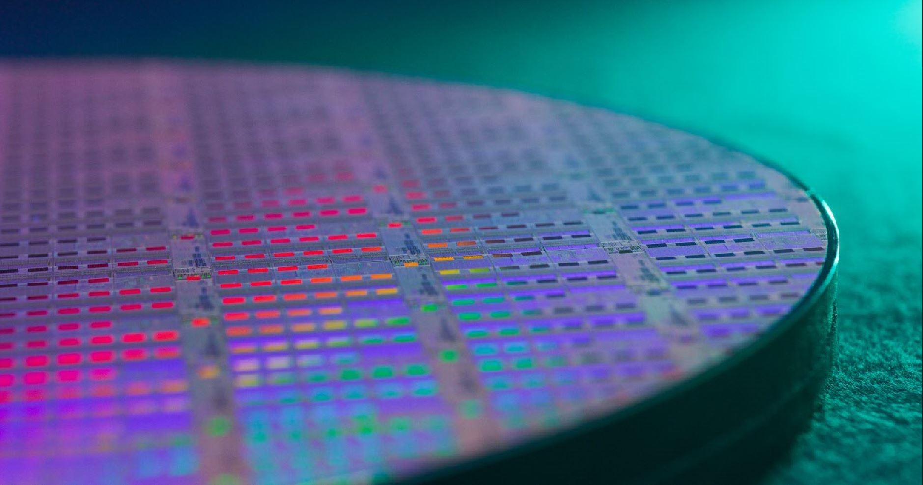
Ayar Labs TeraPHY optical I/O wafer from GlobalFoundries Fotonix
 monolithic RF-CMOS platform. Courtesy of Ayar Labs, 2023
MV: Optical I/O performance enables xPUs to communicate with each other across a wide range of distances, from millimeters up to two kilometers. Therefore, intense competition is expected between AOC (Ethernet) and optical I/O (CXL, UCIe). How will the battle between these two technologies play out?
TT: There is a clear distinction between Ethernet applications and compute or memory-centric applications, so we do not view AOC as a direct competitor. Within the compute or memory-centric interconnect protocols, Compute Express Link (CXL) and Universal Chiplet Interconnect Express
 (UCle
(UCle ) are complementary. CXL is a higher-layer protocol that traditionally runs on a PCIe physical layer. Recently, CXL has been expanded to also work with a UCIe physical layer. For off-chip connectivity within racks or across racks, UCIe optical retimers built using optical I/O technology can deliver low power, low latency, and high bandwidth density metrics that cannot be met with AOC.
With optical interconnects, we can achieve greater reach with lower power consumption and latency. There will still be non-latency-sensitive applications that can accommodate higher power requirements, and Ethernet will be the preferred choice, including system-to-system communications. In these instances, AOC could be used. But once you start considering deep learning and HPC application – where, again, you are connecting many compute nodes together – AOC may not meet all the performance metrics.
MV: How do you see the evolution of optical I/O in terms of technology?
TT: First and foremost, optical I/O is highly scalable and there are several ways the technology will evolve. One is in the number of lambdas per fiber. We are currently using eight lambdas per fiber, but the CW-WDM MSA (Continuous-Wave Wavelength Division Multiplexing Multi-Source Agreement) roadmap already has specifications for 16 and 32 lambdas per fiber. Every time you double the number of lambdas per fiber – keeping everything else the same – you automatically double the amount of bandwidth. We can also scale up the number of optical ports (we are currently using eight) and increase the modulation rates (we are currently using a modulation rate of 32 Gbps).
Within optical I/O, we expect to see a divergence in the use of internal or external lasers. We continue to prefer the external laser approach given the compact form factor, flexibility, and field replaceability. We also believe UCIe is the best-suited standard for die-to-die connectivity, which fosters the chiplet approach of implementing optical I/O.

A multi-chip package with four Ayar Labs TeraPHY optical I/O chiplets and a customer’s ASIC. Courtesy of Ayar Labs, 2023
MV: What are the key specifications around laser sources? Will we see widely integrated lasers in optical chiplets in the future?
TT: The current trend in the industry, and one we believe will continue, is the use of external laser sources. In optical I/O, the laser is the most sensitive component and needs to operate in a cooler temperature environment. Keeping it external and separate from the compute silicon allows you to better and more efficiently control the temperature. If you were to put the laser module next to the compute silicon, the heat coming from the GPUs and CPUs inside the compute node could impact the laser performance.
We do expect to see the use of comb lasers but they are still in the early research stage of development. It is something we could take a look at when the technology becomes commercially available. But, ultimately, we believe remaining ‘external laser agnostic’ makes the most sense in terms of manufacturing and deployment.
MV: There have been many discussions on disaggregated rack architecture, currently the main driver of optical I/O technology. Could you share how disaggregation will evolve?
TT: Disaggregated infrastructure needs optical I/O to scale to the rack level and beyond. Disaggregated architectures that decouple memory from processors and accelerators allow for more flexible and cost-effective node designs that can meet the demands of next-generation HPC and AI workloads. For disaggregation to be possible, an interconnect that can deliver high throughput at low power and low latency over distances ranging from a few meters to hundreds of meters is critical. CXL, an emerging unified protocol for disaggregated systems, uses PCIe electrical signaling for I/O interconnect which has limited reach. To extend the reach and fanout, there is strong interest for a “CXL over optical” I/O interconnect.
For example, it is easy to envision a composability scenario in which several CPUs are contained in one chassis, and the GPUs are in a separate chassis while memory occupies another. As workloads scale up, you can compose two CPUs, one GPU, several SSDs and pool some amount of memory to create one node. CXL brings cache coherent interconnect to memory disaggregation, which is why so many companies are working towards solutions that leverage CXL – and we believe optical I/O is a key ingredient to enable that vision.
Another important angle here is distributed computing, which goes back to the fact that AI/ML and deep learning all require a massive amount of training parameters — now in the trillions. Sharing the computation and memory between various compute nodes will be increasingly necessary. The only reliable way to connect these nodes and scale efficiently is through optical I/O.

Four Ayar Labs TeraPHY optical I/O chiplets and a customer’s ASIC in a multi-chip package. Courtesy of Ayar Labs, 2023
In addition to packaging with chiplets, fiber attach and test methodologies need to evolve. We are also seeing strong progress and commitment from the foundries – namely GlobalFoundries, Intel, and most recently, TSMC – in supporting integrated electro/optical components. Lastly, choosing to keep the lasers external is one way we are able to alleviate these supply chain complexities.
Standardization will also play a key role in addressing supply chain challenges and scaling this technology. Both UCIe and CXL are looking to address interconnects over optical fiber and are exploring the formulation of optical I/O specifications. Further, the CW-WDM MSA is a critical industry initiative that is defining and promoting new standards and specifications for optical laser sources. There is a tremendous need to develop and nurture this full ecosystem because optical I/O is such a revolutionary technology impacting so many areas of the industry.
MV: How will optical I/O technology affect other applications?
TT: That is a great question. We have talked a lot about HPC and AI/ML already, but we also expect to see its use grow in other areas that require the rapid transfer of data such as in the cloud and datacenter, telecommunications, aerospace and defense, autonomous driving, AR/VR and more. As optical I/O matures and becomes even more cost-effective, we see the potential for it to meet the growing bandwidth, power and latency requirements of a wide range of applications.
Acronyms
- AI : Artificial intelligence
- HPC : High-performance computing
- CPO : Co-packaged optics
- CAGR : Compound annual growth rate
- I/O : Input/output
- ML : Machine learning
- xPU : Silicon chip – processing unit has different architectures: CPU, DPU, GPU, TPU, FPGA, ASIC
Featured image: Ayar Labs TeraPHY optical I/O wafer from GlobalFoundries’ Fotonix
 monolithic RF-CMOS platform. Courtesy of Ayar Labs, 2023
The post Leveraging Optical Chip-to-chip Connectivity to Unleash the Complete Potential of AI appeared first on Edge AI and Vision Alliance.


