Desktop simulation of MIT.nano die bonder enables virtual tool training
Digital twins to expand training capabilities through virtual reality.
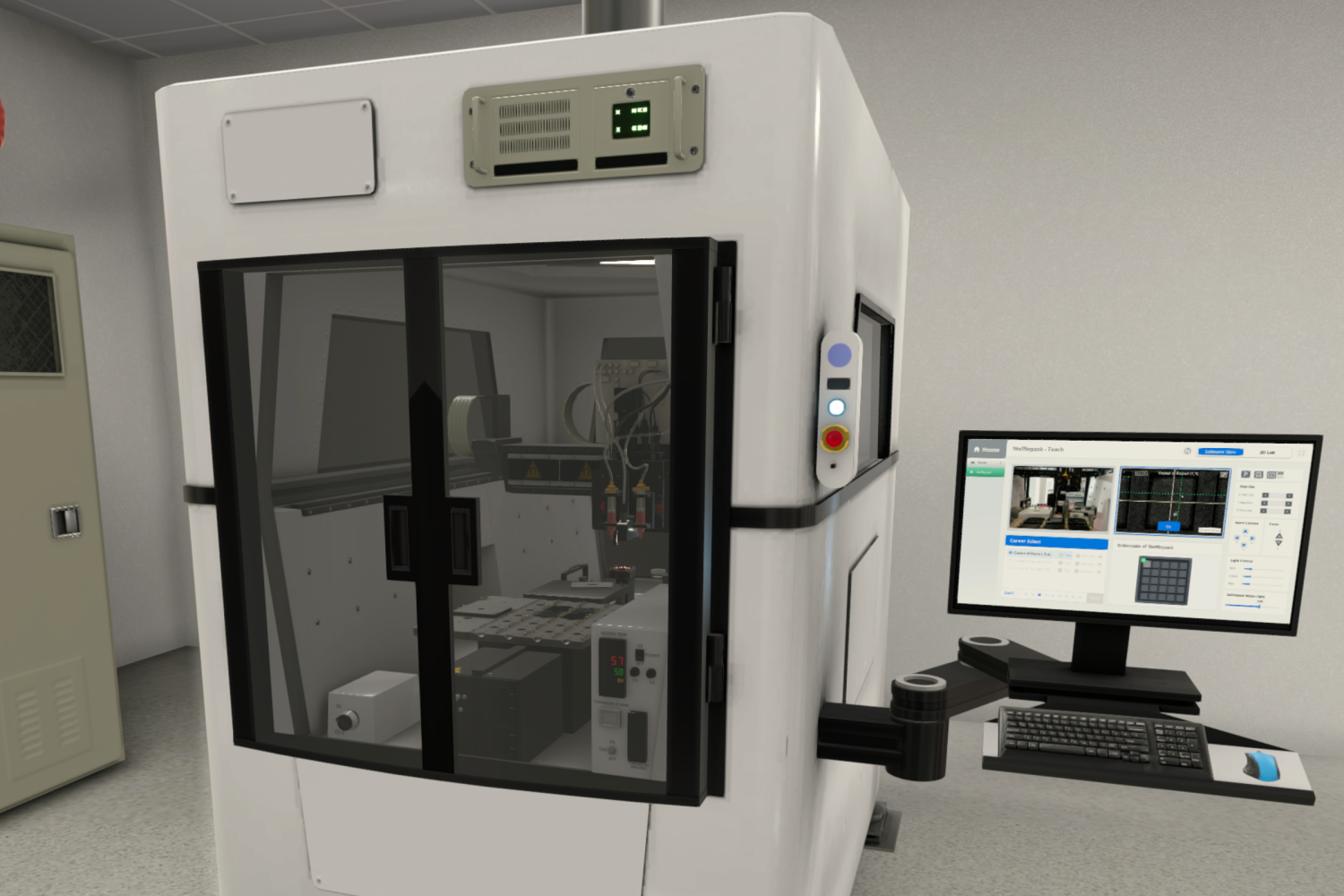
Packaging is the final step in the process for manufacturing a semiconductor device. A critical tool for packing is the die bonder, which facilitates device assembly typically by attaching a chip in a precise location on a substrate.
Die bonders are complicated and can be tricky to learn, but students and technicians all over the world can now practice operating one using a desktop virtual reality (VR) training simulation based on the die bonder located in the Lab for Education and Application Prototypes (LEAP) on the fifth floor of MIT.nano.
The simulation allows trainees to use the tool’s controls to practice lifting and placing semiconductors and glass substrates, and to zoom into the inner workings of the machine, capturing angles and views that sometimes aren’t possible during training with the physical instrument.
The die bonder is one of 40 simulations of advanced manufacturing tools planned for the Virtual Manufacturing Lab (VM-Lab), a three-year collaboration between researchers at MIT, Clemson University, and the University of Arizona. Erik Verlage, a research scientist in the MIT Department of Materials Science and Engineering (DMSE) and the VM-Lab project lead, collaborated with Anu Agarwal, MIT principal research scientist at the Materials Research Laboratory (MRL) and leader of LEAP, and Sri Priya Sundararajan, an industry consultant who is the project manager for the simulation. The project is funded by the Office of Naval Research.
The researchers believe VR tool training could help address the skills gap facing U.S. workers in this sector by making specialized training more widely available and by better preparing users for when they get hands-on training with physical tools.
Simulations democratize access, says Sundararajan. “People will be able to learn a very useful industrial skill that, if they put it on their resume, will make them more attractive as job candidates through the use of this VR simulation.”
A LEAP to VR
The first training modules created by the VM-Lab focused on optical fiber manufacturing at Clemson University. When the time came to work on additional simulations, Agarwal thought the laboratories at MIT.nano contained tools that would contribute to the project’s goals. “The VM-Lab aims to expand access to training,” says Agarwal. “The die bonder is a complicated but standard electronic and photonic packaging tool, and several tools in MIT.nano fall into this same category.”
For machines like the die bonder, engineers and technicians must typically go on-site for training. On-site training is intensive because it is compressed into a short period of time. It’s also expensive because of lost production time on the machine in industry, not to mention the potential costs if a new company employee or student accidentally damages the equipment or the fragile semiconductors in a university teaching lab.
“We wanted to develop a training process such that when students went on-site, they would already have the primer on the fundamentals before they arrived,” says Sundararajan.
Perhaps fittingly, the team that developed the die bonder simulation was a far-flung crew. Several members have never, or rarely, seen the LEAP die bonder in person. Drew Weninger, a third-year graduate student in DMSE professor Lionel Kimerling’s Electronic Materials Group (EMAT), was the eyes and ears for the team, demonstrating the die bonder over Zoom and taking photos and videos of the machine from every angle. Weninger recently saw his work pay off: “I noticed during a boot camp that students who learned from the die bonder simulation before they were trained on the physical tool were not overwhelmed with the terminology, software, and hardware, compared to those who did not have the simulation experience.”
Karina Martínez-Reyes, a summer research scholar in MRL, and a National Science Foundation Research Experience for Undergraduates scholar from the Interamerican University of Puerto Rico, helped write the storyboards and list of parts for the project, with help from the machine’s manufacturer. “Karina could not travel to MIT for her internship due to the pandemic, so she learned about the tool entirely from live simulations provided by Drew,” Agarwal recalls. “And if it worked for her, we were confident it would work to train a remote user.”
An extensive redesign of the graphical user interface by the VM-Lab team helps learners navigate the tool hardware in the VR environment with ease. Kenan Cicek, a DMSE Fulbright scholar, integrated the MIT data and ported it to the Clemson University Center for Workforce Development team, who created the VR simulation. “Co-leading a multi-disciplinary team was a great learning experience,” says Cicek. “The end result was heartwarming when learners, both engineers and technicians, benefited from the tool simulation.”
Training for the future
One of the goals of the VM-Lab is to study how students interact with the simulations and whether they can help cut down on training time. Previous studies show that interactive visualizations are more impactful than text explanations or even videos, Verlage says. “Students report liking these better and feeling more confident when they get to the actual tool.”
In the next steps of the project, Verlage and his colleagues will expand the simulations to resemble something approaching an educational game. Instead of following a step-by-step procedure, the simulation will allow students to explore the tool and use it in their own way to accomplish a specified goal, he says.
Eventually the simulations may use immersive headset virtual reality tools and haptic feedback body suits, Verlage adds. “We would love to start working on the fundamental research of trying to actually make these simulations be a little more tactile, using the equipment at the MIT.nano Immersion Lab.”

